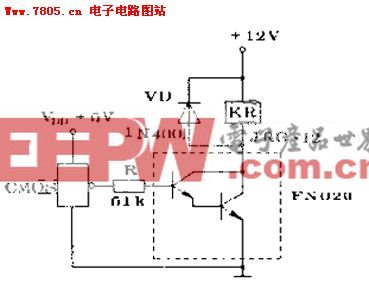
電腦主板PCI槽轉正負12V、5V、5A電流輸出的電路

Figure 1 shows a typical application using the LTC1421.
The LTC1421 works best with a staggered, 3-level connector.
Ground makes connection first to discharge any static
build-up. VCC, VDD and VEE make connection second and
the data bus and all other pins last. The connection sense
pins CON1 and CON2 are located on opposite ends of the
connector to allow the board to be rocked back and forth
during insertion.
,LTC and LT are registered trademarks of Linear Technology Corporation.
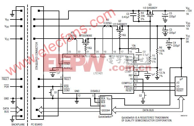
The power supplies on the board are controlled by placing
external N-channel pass transistors Q1, Q2 and Q3 in the
power path for VCC, VDD and VEE, where VCC and VDD can
range from 3V to 12V, and VEE from C 5V to C 12V. By
ramping up the voltage on the pass transistors’ gates at a
controlled rate, the transient surge current [I = (C)(dv/dt)]
drawn from the main backplane supply will be limited to a
safe value. The ramp rate is set by the value of capacitor C2.
The board’s data bus is buffered by a QS3384 QuickSwitch
from Quality Semiconductor. Disabling the QuickSwitch
via the DISABLE pin during board insertion and removal
prevents corruption of the system data bus.
Resistors R1 and R2 form an electronic circuit breaker
function that protects against excessive supply current.
When the voltage across the sense resistor is greater than
50mV for more than 20ms, the circuit breaker trips, immediately
turning off Q1 and Q2 while the FAULT pin is pulled
low. The device will remain in the tripped state until the POR
pin is pulsed low or the power on VCCLO and VCCHI is cycled.
The circuit breaker can be defeated by shorting VCCLO to
SETLO and VCCHI to SETHI.
The RESET signal is used to reset the system microcontroller.
When the voltage on the VOUTLO pin rises above
the reset threshold, PWRGD immediately goes high and
RESET goes high 200ms later. When the VOUTLO supply
voltage drops below the reset threshold, PWRGD immediately
goes low, and RESET goes low 60ms later, allowing
the PWRGD signal to be used as an early warning that a
reset is about to occur. When the FB is left floating, the reset
threshold is 4.65V; when the FB pin is tied to VOUTLO, the
reset threshold is 2.90V.
The uncommitted comparator and internal voltage reference,
along with resistors R6 and R7, are used to monitor
the 12V supply. When the supply drops below 10.8V, the
COMPOUT pin will go low. The comparator can be used to
monitor any voltage in the system.
Push-button switches S1 and S2 are used to generate a
hard and soft reset, respectively. A hard or soft reset may
also be initiated by a logic signal from the backplane.
Pushing S1 shorts the POR pin to ground, generating a
hard reset that cycles the board’s power. Pass transistors
Q1 to Q3 are turned off and VOUTLO and VOUTHI are actively
pulled to ground. When VOUTLO discharges to within 100mV
of ground, the LTC1421 is reset and a normal power-up
sequence is started.
Pushing S2 shorts the FB pin to ground, generating a soft
reset that doesn’t cycle the board’s power. PWRGD immediately
goes low, followed 64ms later by RESET. When S2 is released, PWRGD immediately goes high, followed 200ms
later by RESET.
Board Insertion Timing
When the board is inserted, GND pin makes contact first,
followed by VCCHI and VCCLO (Figure 2, time point 1).
DISABLE is immediately pulled high, so the data bus switch
is disabled. At the same time CON1 and CON2 make contact
and are shorted to ground on the host side (time point 3).
When CON1 and CON2 are both forced to ground for more
than 20ms, the LTC1421 assumes that the board is fully
connected to the host and power-up can begin. When
VCCLO and VCCHI exceed the 2.45V undervoltage lockout
threshold, the 20mA current reference is connected from
RAMP to GND, the charge pumps are turned on and CPON
is forced high (time point 4). VOUTHI and VOUTLO begin to
ramp up. When VOUTLO exceeds the reset threshold voltage,
PWRGD will immediately be forced high (time point
5). After a 200ms delay, RESET will be pulled high and
DISABLE will be pulled low, enabling the data bus (time point 6).

DIY機械鍵盤相關社區:機械鍵盤DIY
基爾霍夫電流相關文章:基爾霍夫電流定律
電流傳感器相關文章:電流傳感器原理


評論