SupertexMD1715和TC8020高清醫療超聲圖像解決方案

Supertex公司的 MD1715和TC8020是高清醫療超聲圖像應用芯片組。MD1715是兩路五級高壓高速脈沖發送芯片,采用先進的CMOS技術,±4.5 到12.5V工作電壓,輸出電流2A,1nF負載的上升和下降時間6.5ns,傳輸時延10ns,1.8V-3.3V CMOS邏輯電平,而TC8020由六對高壓低閾值N溝和P溝MOSFET組成,集成了柵極-源極電阻和齊納二極管,50V時的峰值電流+/-3.5A。本文介紹了MD1715和TC8020主要特性。MD1715和TC8020典型應用電路,以及詳細電路圖。
本文引用地址:http://www.czjhyjcfj.com/article/198900.htmThe Supertex MD1715, paired with the Supertex TC8020, forms a two channel, five level, high voltage, high speed transmit pulser chip set. The chip set is designed for medical ultrasound imaging applications, but can also be used for metal flaw detection, nondestructive evaluation, and piezoelectric transducer drivers.
The MD1715 is a two channel logic controller circuit with 12 low impedance MOSFET gate drivers. There are two sets of control logic inputs, one each for channels A and B. Each channel consists of three pairs of MOSFET gate drivers. These drivers are designed to match the drive requirements of the Supertex TC8020.
The TC8020 is the output stage of the pulser, with six pairs of MOSFETs. Each pair consists of a P-channel and an N-channel MOSFET. They are designed to have the same impedance and can provide typical peak currents of ±3.5 amps at 200V.
MD1715主要特性:
Advanced CMOS technology
±4.5 to 12.5V power supply voltage
2A output source and sink current
6.5ns rise and fall time with 1nF load
10ns propagation delay
±2ns matched delay times
12 matched channels
1.8V to 3.3V CMOS logic interface
Smart logic threshold
Low inductance package
MD1715應用:
Medical ultrasound imaging
Piezoelectric transducer drivers
Metal flaw detection
Nondestructive evaluation
The Supertex TC8020 consists of six pairs of high voltage, low threshold N- and P-channel MOSFETs in a 56-lead QFN package.
All MOSFETs have integrated gate-to-source resistors and gateto-source Zener diode clamps which are desired for high voltage pulser applications. The complimentary, high-speed, high voltage, gate-clamped N- and P-channel MOSFET pairs utilize an advanced vertical DMOS structure and Supertex’s well-proven silicon-gate manufacturing process. This combination produces a device with the power handling capabilities of bipolar transistors and with the high input impedance and positive temperature coefficient inherent in MOS devices.
Characteristic of all MOS structures, this device is free from thermal runaway and thermally-induced secondary breakdown. Supertex’s vertical DMOS FETs are ideally suited to a wide range of switching and amplifying applications where very low threshold voltage, high breakdown voltage, high input impedance, low input and output capacitance, and fast switching speeds are desired.
TC8020主要特性:
High voltage, vertical DMOS technology
Integrated gate-to-source resistor
Integrated gate-to-source Zener diode
Typical peak output +/-3.5A at 50V
Low threshold, low on-resistance
Low input output capacitance
Fast switching speeds
Electrically isolated N- and P-MOSFET pairs
TC8020應用:
High voltage pulsers
Amplifiers
Buffers
Piezoelectric transducer drivers
General purpose line drivers
Logic level interfaces
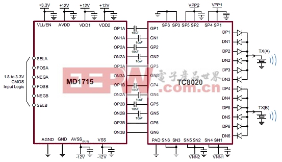
圖1。MD1715和TC8020典型應用電路
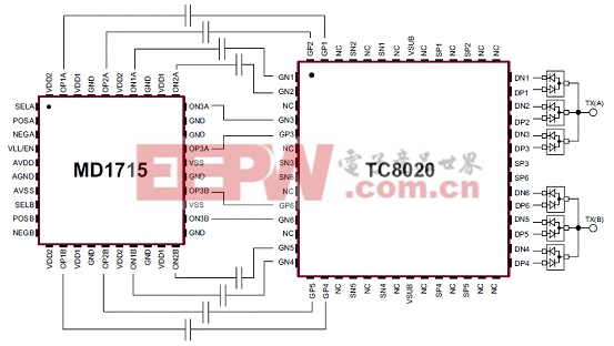
圖2。MD1715和TC8020引腳布局圖
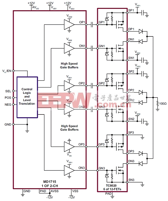
圖3。MD1715和TC8020詳細電路圖
更多醫療電子信息請關注:21ic醫療電子頻道


評論