OnSemiNCP1631300WSLIMLCDTV電源解決方案

The NCP1631 integrates a dual MOSFET driver for interleaved PFC applications. Interleaving consists of paralleling two small stages in lieu of a bigger one, more difficult to design. This approach has several merits like the ease of implementation, the use of smaller components or a better distribution of the heating.
Also, Interleaving extends the power range of Critical Conduction Mode that is an efficient and cost?effective technique (no need for low trr diodes). In addition, the NCP1631 drivers are 180??phase shift for a significantly reduced current ripple.
Housed in a SOIC16 package, the circuit incorporates all the features necessary for building robust and compact interleaved PFC stages, with a minimum of external components.
NCP1631主要特性:
??Near?Unity Power Factor
??Substantial 180 Phase Shift in All Conditions Including Transient Phases
??Frequency Clamped Critical Conduction Mode (FCCrM)i.e.Fixed Frequency, Discontinuous Conduction Mode Operation with Critical Conduction Achievable in Most Stressful Conditions
??FCCrM Operation Optimizes the PFC Stage Efficiency Over the Load Range
??Out?of?phase Control for Low EMI and a Reduced rms Current in the Bulk Capacitor
??Frequency Fold?back at Low Power to Further Improve the Light Load Efficiency
??Accurate Zero Current Detection by Auxiliary Winding for Valley Turn On
??Fast Line / Load Transient Compensation
??High Drive Capability: ?500 mA / +800 mA
??Signal to Indicate that the PFC is Ready for Operation (“pfcOK” Pin)
??VCC Range: from 10 V to 20 V
NCP1631安全特性:
??Output Over and Under Voltage Protection
??Brown?Out Detection with a 50?ms Delay to Help Meet Hold?up Time Specifications
??Soft?Start for Smooth Start?up Operation
??Programmable Adjustment of the Maximum Power
??Over Current Limitation
??Detection of Inrush Currents
NCP1631應用:
??Computer Power Supplies
??LCD / Plasma Flat Panels
??All Off Line Appliances Requiring Power Factor Correction

圖1.NCP1631功能方框圖
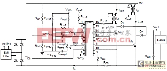
圖2.NCP1631典型應用電路圖
300W SLIM LCD TV電源參考設計
This reference document describes a built-and-tested, GreenPoint? solution for an LCD-TV power solution that combines the main system power without a backlight power converter. In this architecture, the backlight power converter is designed on a separated board to allow full design flexibility and easier adaptation to any backlight solution and technology (Classical 24 V Hall Bridge resonance Power Supply or LIPS / High Voltage Inverter for CCFL, Power converter for Fronts or Edge LED Backlight or finally Power converter for PDP /Plasma panel).
This reference design circuit consists of a 290 mm x 310 mm printed circuit board designed to fit into the chassis of a Flat-TV. The height is limited to 8 mm to allow advanced Slim low depth LCD TV design. All the circuitry is resident in on a single-sided PCB as might be found on an LCD-TV but with FR4 / Glass Epoxy material. This allows large holes in the PCB without adding issues in drop or vibration tests.
The low profile design has a direct impact on the passive component definitions.
The overall winding parts (common mode EMI filters, PFC coils, Standby and Flyback transformers) have been defined with a low profile ferrite core and a new bobbin, allowing the parts to be lower than 8 mm with holes in the PCB included.
The large electrolytic capacitors have been split into multiple lower values and inserted flat on the board. They measure a diameter of 10 mm, and also include holes in the PCB. The heat sinks have been designed with a new low profile allowing them to be below 7 mm.
The ON Semiconductor devices utilized are from the latest generation of controllers. This design has been engineered to achieve optimum performance compared to traditional LCD-TV power architectures, while simplifying the overall bill of materials. This is done by selecting a proprietary high performance low power mode standby integrated switcher, a high efficiency interleaved Frequency Clamp Critical Conduction Mode (FCCrM) PFC, and a Flyback controller topology that provides the power to the overall TV signal processing and audio amplifiers. To provide higher design flexibility, 2 types of Flyback controllers have been considered requiring minimal changes to move from one to the other. The first one is a new Quasi Resonance (QR) mode while the second is a fixed frequency PWM.

圖3.300W SLIM LCD TV電源參考設計外形圖
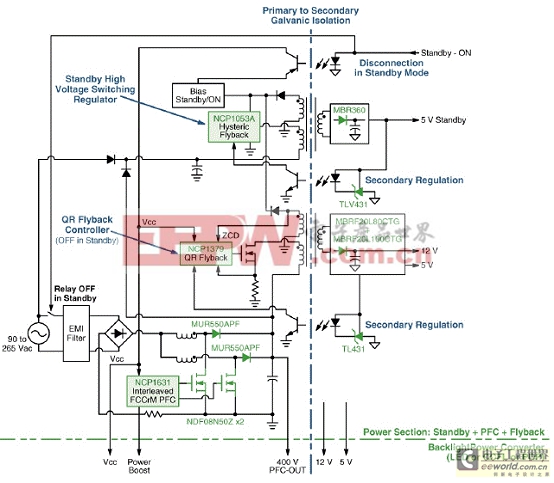
圖4.300W SLIM LCD TV電源參考設計方框圖

圖5. 8毫米SLIM 主濾波器和PFC電路圖

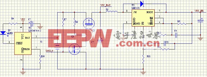
圖6. 8毫米SLIM ECO待機電源電路圖

圖7. 8毫米SLIM QR反激電源電路圖
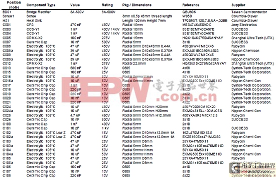
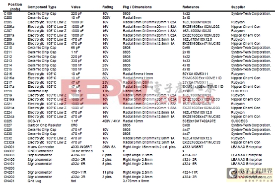
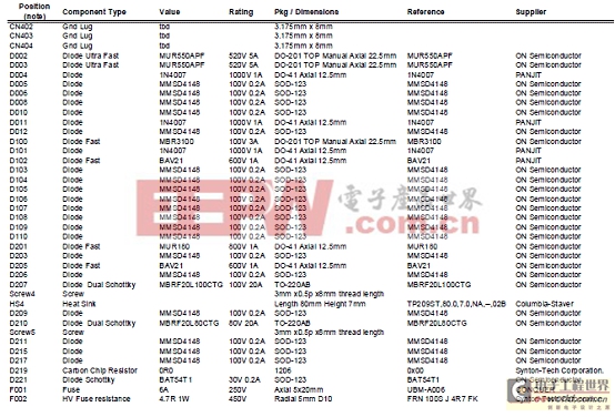
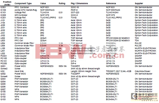
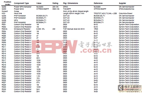
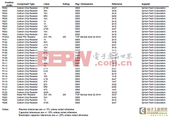
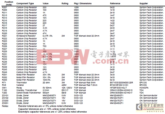
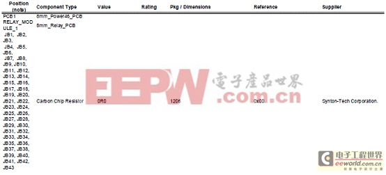
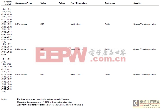
300W 8毫米LCD TV電源材料清單:
詳情請見K
詳情
詳情請見:
http://www.onsemi.cn/pub_link/Collateral/NCP1631-D.PDF
和
http://www.onsemi.cn/pub_link/Collateral/TND401-D.PDF

LCD顯示屏相關文章:lcd顯示屏原理
lcd相關文章:lcd原理


評論