PowerintTOP270VG100W小型反激電源解決方案

TOPSwitch-JX cost effectively incorporates a 725 V power MOSFET, high-voltage switched current source, multi-mode PWM control, oscillator, thermal shutdown circuit, fault protection and other control circuitry onto a monolithic device.
TOPSwitch-JX系列產(chǎn)品亮點(diǎn):
EcoSmart – Energy Effi cient
? Ideal for applications from 10 W to 245 W
? Energy efficient over entire load range
? No-load consumption below 100 mW at 265 VAC
? Up to 750 mW standby output power for 1 W input at 230 VAC
High Design Flexibility for Low System Cost
? Multi-mode PWM control maximizes effi ciency at all loads
? 132 kHz operation reduces transformer and power supply size
? 66 kHz option for highest effi ciency requirements
? Accurate programmable current limit
? Optimized line feed-forward for line ripple rejection
? Frequency jittering reduces EMI fi lter cost
? Fully integrated soft-start for minimum start-up stress
? 725 V rated MOSFET
? Simplifi es meeting design derating requirements
Extensive Protection Features
? Auto-restart limits power delivery to 3% during overload faults
? Output short-circuit protection (SCP)
? Output over-current protection (OCP)
? Output overload protection (OPP)
? Output overvoltage protection (OVP)
? User programmable for hysteretic/latching shutdown
? Simple fast AC reset
? Primary or secondary sensed
? Line undervoltage (UV) detection prevents turn-off glitches
? Line overvoltage (OV) shutdown extends line surge withstand
? Accurate thermal shutdown with large hysteresis (OTP)
Advanced Package Options
? eDIP?-12 package:
? 43 W / 117 W universal input power output capability with
PCB / metal heat sink
? Low profi le horizontal orientation for ultra-slim designs
? Heat transfer to both PCB and heat sink
? Optional external heat sink provides thermal impedance
equivalent to a TO-220
? eSIP?-7C package:
? 177 W universal input output power capability
? Vertical orientation for minimum PCB footprint
? Simple heat sink mounting using clip provides thermal
impedance equivalent to a TO-220
? eSOP?-12 package:
? 66 W universal input output power capability
? Low profi le surface mounted for ultra-slim designs
? Heat transfer to PCB via exposed pad and SOURCE pins
? Supports wave or refl ow soldering
? Extended creepage to DRAIN pin
? Heat sink is connected to SOURCE for low EMI
TOPSwitch-JX系列典型應(yīng)用:
? Notebook or laptop adapter
? Generic adapter
? Printer
? LCD monitor
? Set-top box
? PC or LCD TV standby
? Audio amplifi er
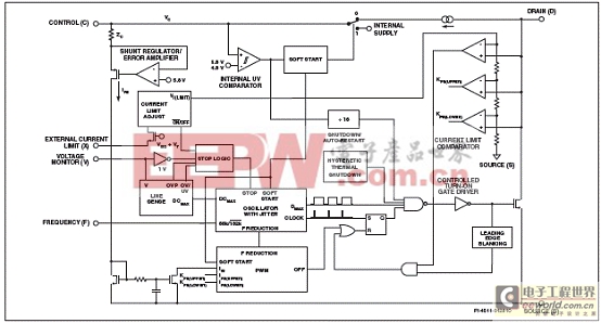
圖1.TOPSwitch-JX系列方框圖
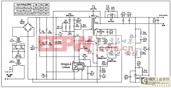
圖2.TOPSwitch-JX系列通用輸入19V 65W反激電源電路圖
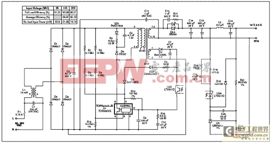
圖3.TOPSwitch-JX系列通用輸入12V 30W反激電源電路圖
12V/24V 100W反激電源評估板
This document is an engineering report describing a 12 V / 24 V, 100 W flyback DC-DC converter utilizing a TOP270VG from the TOPSwitch-JX family of ICs. This power supply is intended for use in an LCD TV with LED back light. The board requires +380 VDC input, supplied from the PFC stage in a typical TV design.
100W反激電源評估板主要特性:
? Highly energy efficient
? Full load efficiency >90%
? Efficiency >89% above 10% load
? Average efficiency >90% (25%, 50%, 75%, 100% load points)
? Simplifies meeting ENERGY STAR 2.0 and EuP requirements
? Low cost, low component count and small PCB footprint solution
? Performance met without synchronous output rectification
? 132 kHz operation optimized core size and efficiency performance
? Low profile eDIP?-12 package for ultra-slim designs
? Integrated protection and reliability features
? Line under voltage lock out (UVLO)
? Primary sensed output overvoltage shutdown (OVP). Latched OVP condition can be reset with a fast AC reset circuit.
? Auto recovery output over current (OCP)
? Meets limited power source (LPS) 100 VA requirement with a single point of failure
? Accurate thermal shutdown with large hysteresis

圖4.100W反激電源評估板外形圖
100W反激電源主要指標(biāo):
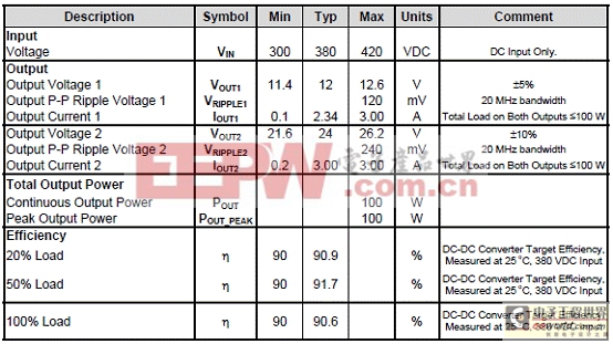
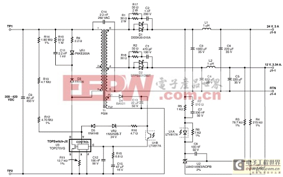
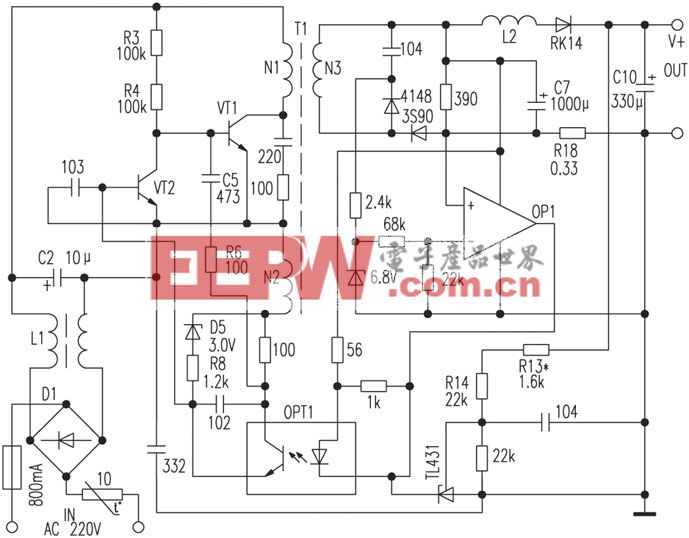
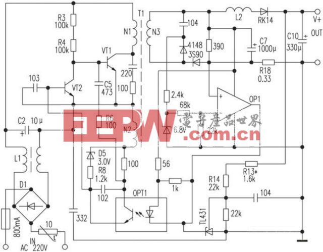
圖5.100W反激電源評估板電路圖
100W反激電源評估板材料清單(BOM):
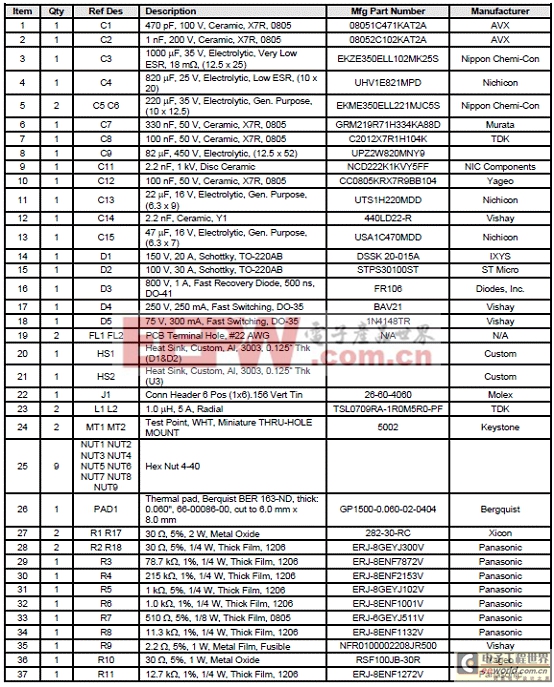
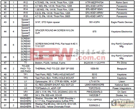
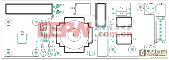
圖6.100W反激電源評估板PCB布局圖(頂層)
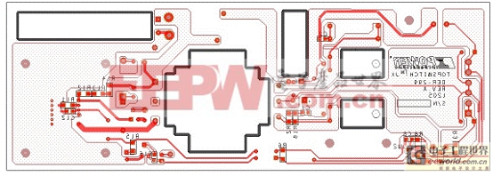
圖7.100W反激電源評估板PCB布局圖(底層)
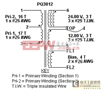
圖8.變壓器電路圖
詳情請見:
http://www.powerint.com/sites/default/files/product-docs/topjx_family_datasheet.pdf
和
http://www.powerint.com/sites/default/files/PDFFiles/der299.pdf

pwm相關(guān)文章:pwm是什么
電路圖符號相關(guān)文章:電路圖符號大全


評論